Advanced chip packaging, printed in a single exposure.
PhaseFab is developing additive manufacturing for advanced semiconductor packaging and beyond; complex, multimaterial 3D structures produced in a single step and at micrometer scale.
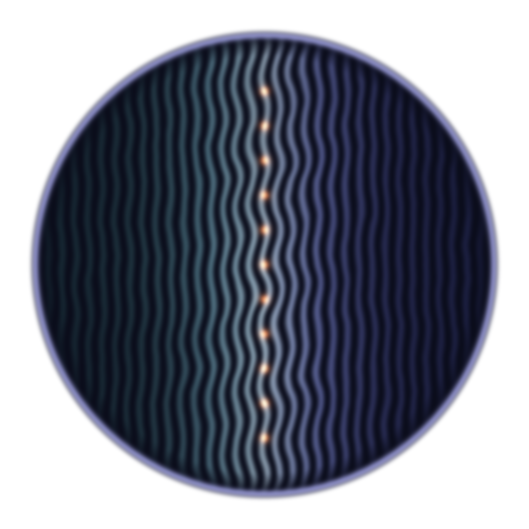

One step. Any shape.
Conventional packaging builds structures layer by layer through dozens of process steps. Our approach uses patterned light to form metal-and-polymer microstructures directly, in three dimensions, all at once.
Single-step, multimaterial
Hybrid metal–polymer resins are patterned holographically into finished 3D structures with no stacking, bonding, or repeated lithography.
Finer than a human hair
Feature resolution below 10 microns supports the dense interconnects advanced chiplet and fan-out packages demand.
Turnaround from months to days
Collapsing multistep package fabrication with >10 tools into one printing step and a simple post process shortens design-to-part cycles from months to days.
The hologram starts as a phase mask.
Every print begins with a greyscale, square-pixel phase mask. Each pixel delays light by a precise amount, and the shaped wavefront interferes into a three-dimensional hologram projected inside the resin. Where the light converges, features are fabricated.
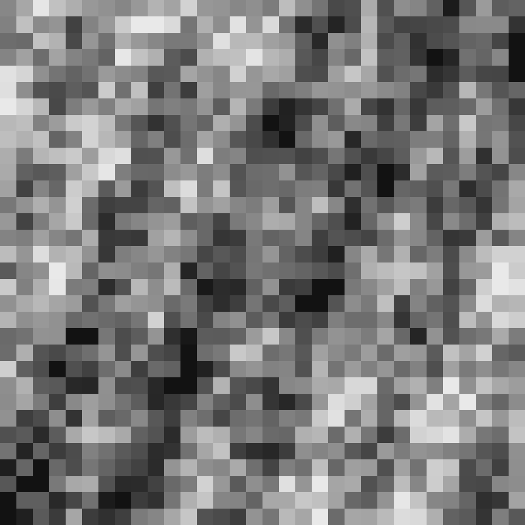 Phase mask
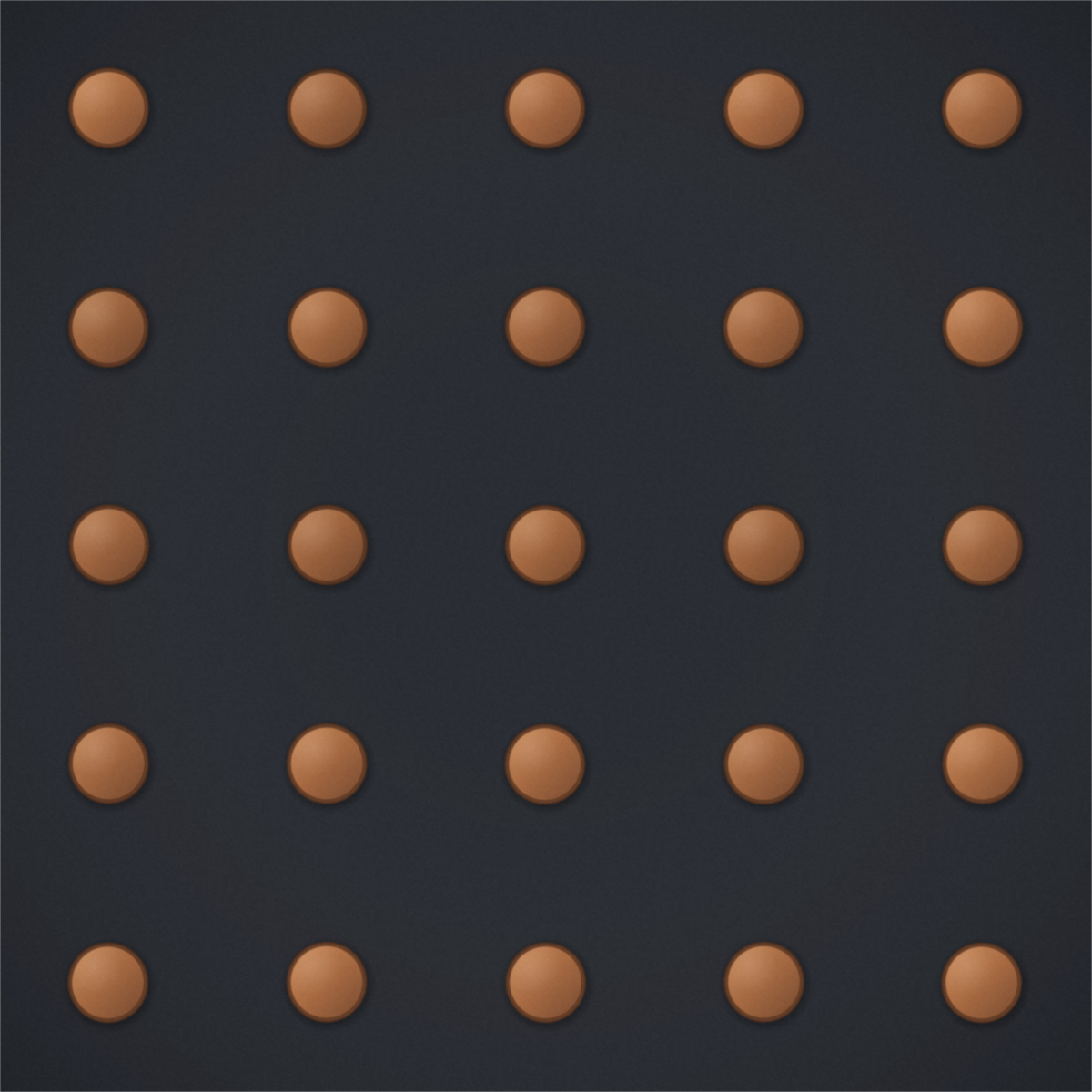 Printed pillar array
Where printed packaging matters
Advanced compute
Dense fan-out and chiplet packages for processors that outgrow planar interconnect.
Aerospace & defense
Rapid, low-volume fabrication of specialized packages without a full production line.
Nonplanar form factors
Curved and conformal packages that traditional flat-wafer processes cannot produce.
Rapid prototyping
Iterate on package designs in days, before committing to volume tooling.